陈蓉教授赴荷兰出席ASD 2017大会并作了关于"Design and synthesis of catalytic nanoparticles via area selective atomic layer deposition"的邀请报告。
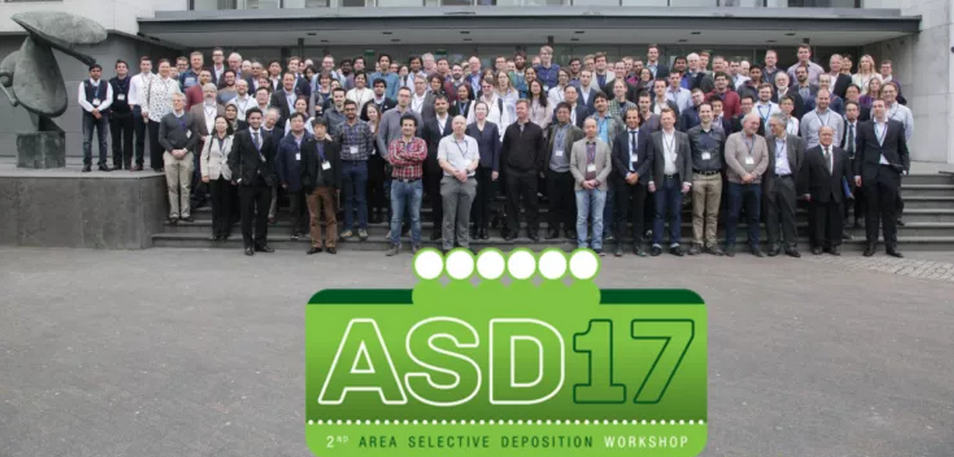
On April 20-21, the 2nd Area Selective Deposition workshop (ASD 2017) took place in Eindhoven. Here we give a brief flashback of the workshop and include several photographs of the meeting, including a group photo of the participants.
The workshop started on Thursday evening with a welcome reception. This reception took place on the campus of the Eindhoven University of Technology (TU/e) and it was a nice gathering where people could see our new Flux building, have a glimpse at our labs, and enjoy good food and drinks. The lab visit was organized in small groups stopping at various stations where they were informed about the research taking place in the Plasma & Materials Processing group. The participants could have a look at our home-built ALD equipment, our furnaces for the preparation of 2D materials, and our NanoLab@TU/e clean room.
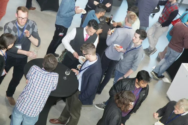
Welcome reception of ASD 2017 taking place at the premises of the Eindhoven University of Technology the evening before the workshop.
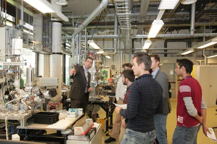
Lab tour through the labs of the Plasma & Materials Processing group. The main organizer of ASD 2017 – Adrie Mackus – shows our home-built ALD equipment that is also used for area-selective deposition.
The actual workshop started in the morning of Friday April 21. The venue was the Pullman hotel in the city center of Eindhoven. The room was well filled. As discussed previously, the number of registrations was quite overwhelming. There were 152 participants with about 55% of those coming from industry. Some companies represented at the workshop are highlighted on the slide below presented during the introduction. It is also clear that the workshop was very international with many participants from the U.S. and the Far East.
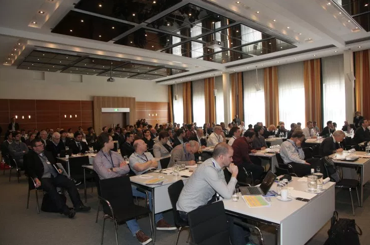
The conference room during ASD 2017 filled with over 150 participants.
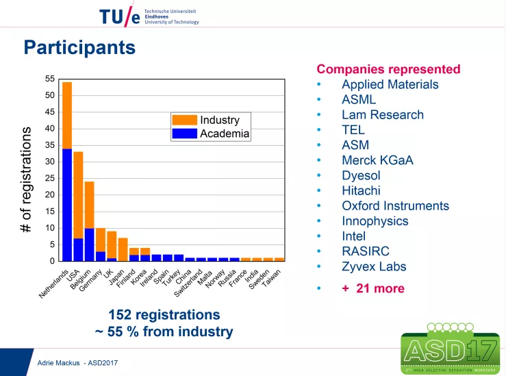
Slide presented during the introduction of the workshop by Adrie Mackus. It underlines the international character of the workshop as well as the large interest in ASD from companies.
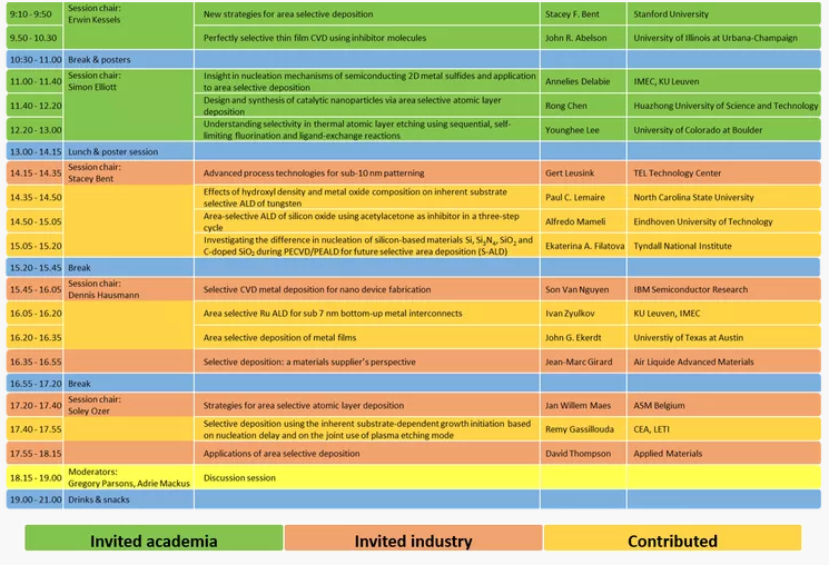
Program of ASD 2017. The program is a mix of invited presentations from academia (40 min. each), invited presentations by industry (20 min. each), contributed presentations (15 min. each) and contributed poster presentations during the breaks. The workshop was concluded with a discussion session and drinks & snacks.
Stacey Bent from Stanford University kicked off the technical program. Stacey is one of the pioneers of area-selective ALD as she and her co-workers published their first paper on area-selective ALD using area-deactivation with self-assembled monolayers (SAMs) already in 2004 (R. Chen et al. Appl. Phys. Lett. 84, 4017 (2004), 10.1063/1.1751211). After a short introduction about the need for selective deposition, Stacey started with this initial work and she subsequently continued with her more recent work on area-selective ALD of dielectric materials on metal/dielectric patterns of SiO2 and Cu. In this work the aim was to push the thickness limit of the selectively deposited dielectrics. For the thiol SAMs used, she addressed the difference between vapor vs. solution deposition showing that vapor deposition yields better results. She also showed that the selectivity is poorer for Al2O3 than for ZnO. Furthermore she introduced two approaches to improve the selectivity: 1) a self-correcting process using chemical etching (F. S. Minaye Hashemi et al., ACS Nano 9, 8710 (2015), 10.1021/acsnano.5b03125); and 2) regeneration of the protective SAM (F. S. Minaye Hashemi and S. F. Bent, Adv. Mater. Interfaces 3, 1600464 (2016), 10.1002/admi.201600464). With the latter, three times thicker ZnO films can be deposited selectively. This means that even films with thicknesses >100 nm can be deposited on SiO2 without depositing on Cu. Next she addressed the question “Does area selective deposition work with Molecular Layer Deposition (MLD)?” Apparently the absorption of MLD precursors in the SAM is an issue here that will need to be addressed. It was also observed that MLD layers peeled off during the selective etching leading to rough pattern edges. Stacey ended her presentation with a short discussion about their work on topographically-selective deposition which was recently published (W.H. Kim et al. ACS Nano, 10, 4451 (2016), 10.1021/acsnano.6b00094).
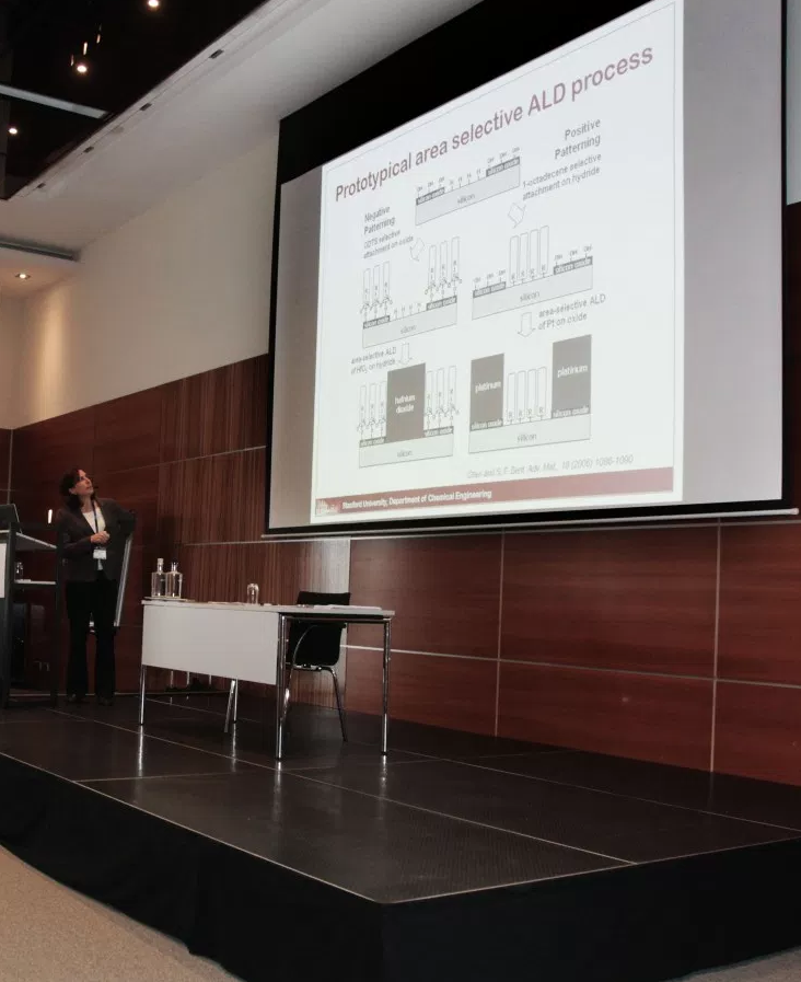
Stacey Bent of Stanford University showing her pioneering work on area-selective ALD using self-assembled monolayers.
John Abelson from the University of Illinois at Urbana-Champaign was the second invited speaker from academia. He took us back to the fundamentals of CVD. He stressed the important role of defects during nucleation and he pointed out the difference between high temperature CVD and low temperature CVD. At low temperature, the surface remains mostly covered with adsorbed precursor, product or inhibitors (if added). Subsequently he addressed how working at high pressures can increase the conformality of a CVD process (in this case HfB2). He also demonstrated that for those cases in which the vapor pressure of the precursor is low, a growth inhibitor can be added (N. Kumar et al., JACS 130, 17660 (2008), 10.1021/ja807802r). It was shown that co-dosing such an inhibitor can 1) improve conformality, 2) reduce surface roughness, or 3) affords selective deposition on specific surfaces. This was illustrated by results on TiB2and Fe. Also consumable inhibitors can be used, for example N and H atoms produced by a plasma source. Finally, John demonstrated that perfect selectivity can be achieved for Cu CVD on RuO2 in the presence of (carbon-doped) SiO2 when using VTMS as inhibitor. (S. Barbar et al., ECS J. Solid State Sci. Technol. 4, N60 (2015), 10.1149/2.0061507jss)

John Abelson from the University of Illinois at Urbana-Champaign talking about the fundamentals of CVD and how growth inhibitors can be used to deposit conformal films and to control nucleation.
Annelies Delabie of IMEC gave a very interesting presentation about the preparation of semiconducting 2D transition metal dichalcogenides and the possibilities with area-selective deposition. She started with a nice overview of the importance of ASD for future technologies in semiconductor fabrication and the many efforts by IMEC currently going on. Then she focused on 2D materials, either prepared by CVD, ALD or MBE (molecular beam epitaxy). It was a very rich and insightful presentation addressing many aspects, ranging from the fundamentals of nucleation to integration schemes. She focused on two topics. The first one being ASD of WS2 using a new concept for selective deposition: conversion of sacrificial patterns. This is an interesting method employing sacrificial Si patterns which are converted into WS2 patterns using a pulsed CVD process at 450 ⁰C. This work has recently been published (M. H. Heyne et al,Nanotechnology 28 04LT01 (2017) 10.1088/1361-6528/aa510c). The second topic she addressed was more fundamental, i.e., the understanding of nucleation mechanisms of CVD and ALD processes. Here she mainly reported on a plasma-enhanced ALD process of WS2 using WF6, H2 plasma and H2S (B. Groven et al, Chemistry of Materials, 29 (7), 2927–2938 (2017)10.1021/acs.chemmater.6b05214). It was discussed how controlling the initial nucleation density affects the final grain size of the 2D material. She also presented results on CVD of SnS and SnS2. The final conclusion was that the seeding of 2D crystals at well-defined locations can be exploited for ASD of 2D materials.
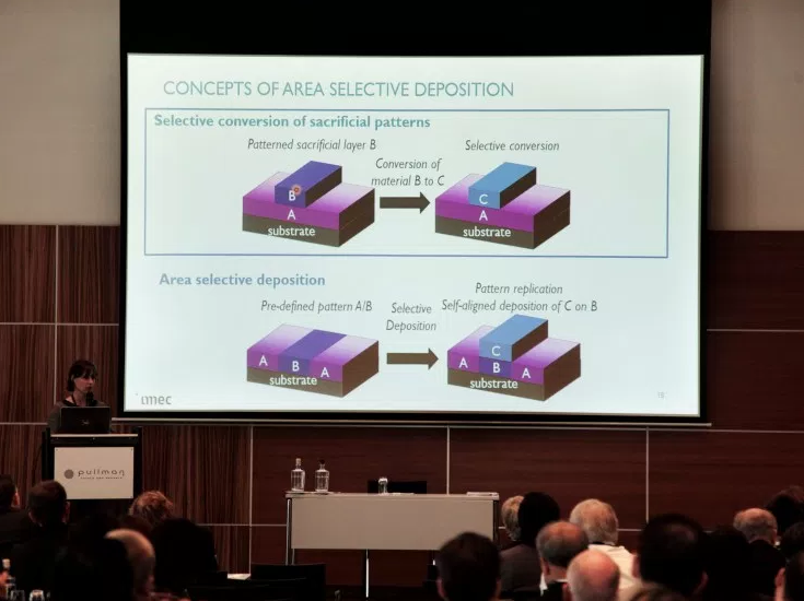
Annelies Delabie from IMEC presenting concepts for bottom-up preparation of patterned 2D materials: 1). Conversion of sacrificial patterns and 2). Area-selective deposition.
With the first three invited presentations being mostly focused on the semiconductor industry, Rong Chen from the Huazhong University of Science and Technology made clear that area-selective ALD has also interesting applications in the field of catalysis. First she pointed out that it is vital to design catalysts for optimized activity, stability and selectivity. Subsequently she addressed that ALD can be used to design catalysts and that area-selective processes provide several opportunities. Area-selective ALD processes can be used to prepare core-shell bimetallic catalysts of noble metals with regular ALD recipes (M.J. Weber et al. Chem. Mater. 24, 2973 (2012),10.1021/cm301206e ). A similar thing can be done by SAMs (K. Cao et al., Sci. Rep. 5, 8470, 2015, 10.1038/srep08470) while such SAMs can also be used to block ALD growth on noble metal particles, such that it is possible to tailor the surface of the metal oxide support material. In this way, basically Co3O4 can be deposited around Pt nanoparticles as a sort of nanotrap (X. Liu et al., Angew. Chem. 129, 1670 (2017), 10.1002/anie.201611559) which leads to a greatly enhanced thermal stability of the Pt nanoparticles. Furthermore, she presented results on so-called facet-selective ALD, i.e. ALD growth that is only obtained at specific facets of the particle. Instead of being dependent on the surface material, such an ALD process is even selective to the crystal orientation. Facet-selective ALD of CeO2 can be used to generate nanofence coatings on Pt nanoparticles. From the results shown, it can be concluded that selective ALD is a powerful synthesis method to create model catalysts.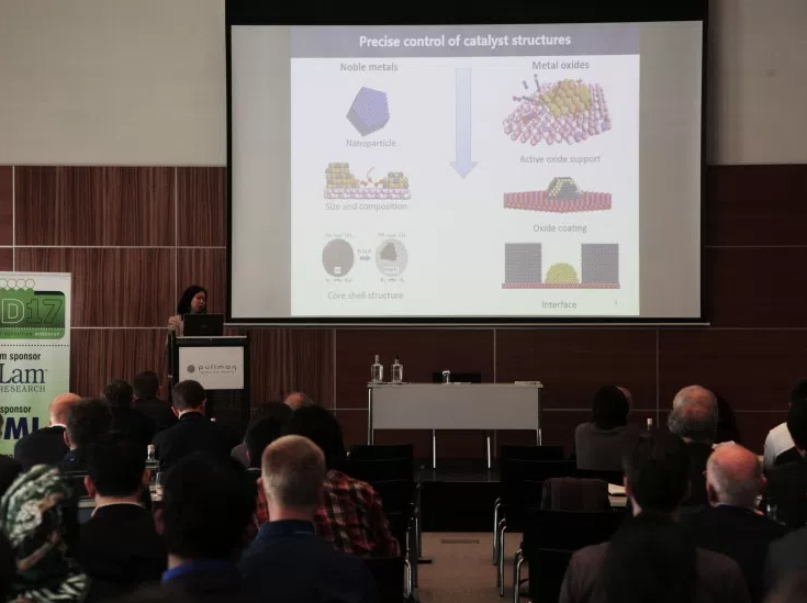
Rong Chen from the Huazhong University of Science and Technology showing that it is possible to precisely control catalyst structures by applying (area-selective) ALD processes.
The last invited presentation from academia was given by Younghee Lee. Working in the group of Steven George at the University of Colorado, he has played a pioneering role in the field of atomic layer etching. The title of his presentation was “Understanding Selectivity in Thermal Atomic Layer Etching Using Sequential, Self-Limiting Fluorination & Ligand-Exchange Reactions”. Atomic layer etching (ALE) is currently also a very hot topic in the field of semiconductor processing as it is considered key for sub-10 nm technology nodes. Besides anisotropic etch processes, it is expected that also isotropic dry etch processes will be required when transitioning to advanced 3D devices such as gate-all-around transistors. The group of Steven George recently introduced real “reverse ALD processes” (S. M. George & Y. Lee, ACS Nano 10, 4880 (2016), 10.1021/acsnano.6b02991). Not surprisingly, ALD and (isotropic) ALE processes have many things in common and obviously selectively has always been a key figure of merit of etch processes. In addition, novel combinations of ASD and selective etching are currently being considered for improving the selectivity of ASD, which makes it even more relevant to look into ALE. Younghee gave an overview of the work done at the University of Colorado on thermal ALE of materials employing self-limiting fluorination by HF pyridine. He first presented the initial work on using Sn(acac)2 as metal reactant that serves as a volatile and reactive fluorine acceptor and he discussed the selectivity that can be obtained by this process (Y. Lee, & S.M. George, ACS Nano 9, 2061 (2015),10.1021/nn507277f). He continued with the more recent work using Al(CH3)3 as metal reactant (Y. Lee, et al., Chem. Mater. 28, 2994 (2016) 10.1021/acs.chemmater.6b00111) and then turned to the selectivity in ALE that can be obtained when using Sn(acac)2, Al(CH3)3, AlCl(CH3)2, and SiCl4 as metal reactants (Y. Lee et al. Chem. Mater. 28, 7657 (2016), 10.1021/acs.chemmater.6b02543). From the results he drew the preliminary conclusion that the selectivity of ALE depends on the stability and volatility of reaction products (Y. Lee, C. Huffman & S.M. George, Chem. Mater. 28, 7657 (2016), 10.1021/acs.chemmater.6b02543). Finally, he demonstrated that reaction temperature forms an additional pathway for achieving selectivity in ALE. This interesting work is certainly “to be continued”.
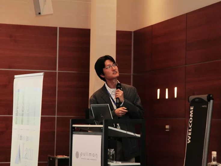
Younghee Lee from the University of Colorado presented his work on thermal atomic layer etching (ALE). He addressed the selectivity that can be achieved with the processes based on self-limiting fluorination and ligand-exchange reactions and he discussed the current level of understanding.
The program in the afternoon of the 1-day workshop consisted of invited presentations by engineers and scientists from industry as well as some contributed presentations chosen on the basis of abstracts submitted. Industry presentations were given by Tokyo Electron, IBM, Air Liquide, ASM and Applied Materials. Although the level of detail given was obviously limited, it was informative how the different companies addressed the topic of area-selective deposition. Gert Leusink from TEL discussed that the patterning paradigm is shifting to self-alignment and bottom-up approaches whereas Son Van Nguyen from IBM reported the state of the art of selective metal CVD processes being (nearly) implemented in fabs. As expected, Jean-Marc Girard from Air Liquide considered ASD from the point of view of precursors while Jan Willem Maes from ASM presented some strategies for area-selective ALD showing a few of the results ASM obtained. Finally David Thompson from Applied Materials gave an instructive and entertaining presentation in which he also highlighted some important (fundamental) aspects of the processes that should not be overlooked. Altogether, the presentations were quite complementary to each other yielding important insight from the industry perspective.
The formal program of the workshop ended with a discussion session led by Adrie Mackus and Greg Parsons. Although it had been a long day and notwithstanding the fact that it was already past 6 pm on a Friday, this discussion was very lively with some animated contributions by some participants. In a future blog, some of the discussion topics will be highlighted, and some general conclusions will be drawn about what the new developments are in the ASD community.
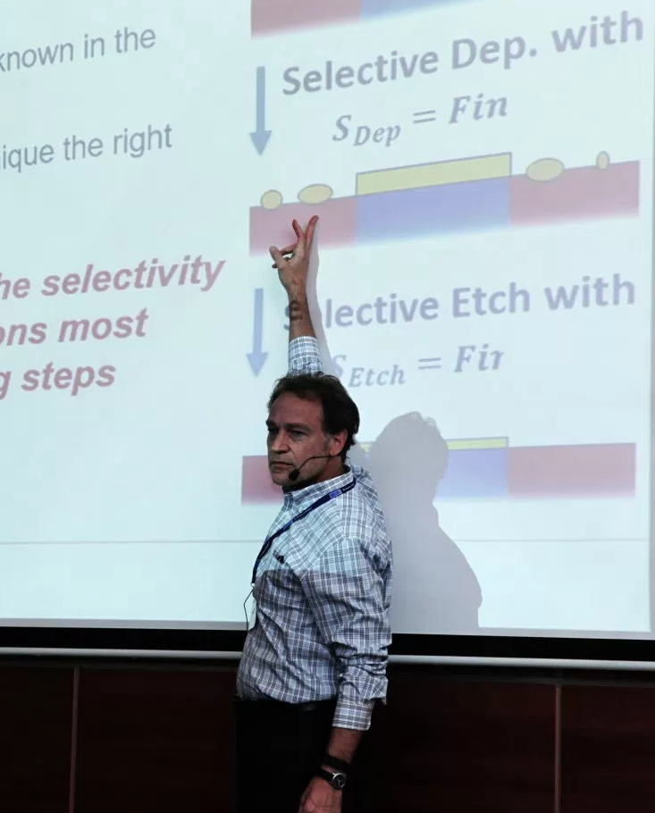
Greg Parsons leading and contributing to the discussion session at the end of the ASD 2017 workshop.
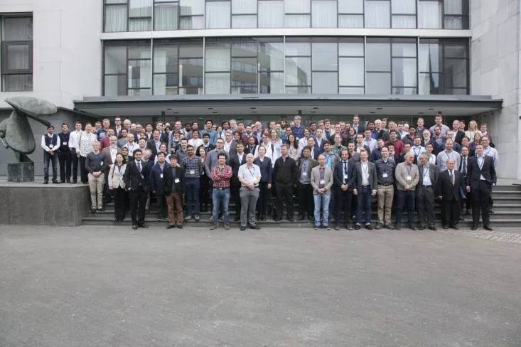
Group photo of the participants of the ASD 2017 workshop in Eindhoven.
We thank Maria Mione for taking these great pictures!
References
- R. Chen et al. Appl. Phys. Lett. 84, 4017 (2004), 10.1063/1.1751211
- F. S. Minaye Hashemi et al., ACS Nano 9, 8710 (2015), 10.1021/acsnano.5b03125
- F. S. Minaye Hashemi and S. F. Bent, Adv. Mater. Interfaces 3, 1600464 (2016), 10.1002/admi.201600464
- W.H. Kim et al. ACS Nano, 10, 4451 (2016), 10.1021/acsnano.6b00094
- N. Kumar et al., JACS 130, 17660 (2008), 10.1021/ja807802r
- M. H. Heyne et al, Nanotechnology 28 04LT01 (2017) 10.1088/1361-6528/aa510c
- B. Groven et al, Chemistry of Materials, 29 (7), 2927–2938 (2017) 10.1021/acs.chemmater.6b05214
- M.J. Weber et al. Chem. Mater. 24, 2973 (2012), 10.1021/cm301206e
- K. Cao et al., Sci. Rep. 5, 8470, 2015, 10.1038/srep08470
- X. Liu et al., Angew. Chem. 129, 1670 (2017), 10.1002/anie.201611559
- S. M. George & Y. Lee, ACS Nano 10, 4880 (2016), 10.1021/acsnano.6b02991
- Y. Lee, & S.M. George, ACS Nano 9, 2061 (2015), 10.1021/nn507277f
- Y. Lee, et al., Chem. Mater. 28, 2994 (2016) 10.1021/acs.chemmater.6b00111
- Y. Lee et al. Chem. Mater. 28, 7657 (2016), 10.1021/acs.chemmater.6b02543
- Y. Lee, C. Huffman & S.M. George, Chem. Mater. 28, 7657 (2016), 10.1021/acs.chemmater.6b02543